|
|
|
|
|
|
|
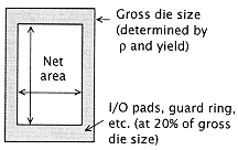
Figure 2.26
Net die area. |
|
|
|
|
|
|
|
|
defect density of one defect per square centimeter; for economic reasons, we target an initial yield of 10%. |
|
|
|
 |
|
|
|
|
Y = e-rDA, |
|
|
|
|
|
|
|
|
where rD = 1 defect/cm2, Y = 0.1. Then |
|
|
|
|
|
|
|
|
In other words, the gross chip area available to us is 230 mm2. This is the total die area of the chip, but such things as pads for the wire bonds that connect the chip to the external world, drivers for these connections, and power supply lines all act to decrease the amount of chip area available to the designer. In general, we allow 20% of the chip areausually around the periphery of the chipto accommodate these functions: |
|
|
|
|
|
|
|
|
Pads + Guard Ring + Pad Drivers + Power Supply |
|
|
|
|
|
|
|
|
= 20% of 230 mm2 = 46mm2. |
|
|
|
|
|
|
|
|
Hence, the net area is 184 mm2. This is the net area available to the microprocessor designer. |
|
|
|
|
|
|
|
|
Feature Size The smaller the feature size, the more logic that can be accommodated within a fixed area. As we discussed earlier, the rbe has been empirically determined to be approximately 2700 l2. Assume we have a process whose minimum feature size is one micron. Therefore, |
|
|
|
|
|
|
|
|
f = 1m |
|
|
|
|
|
|
|
|
f = 2l, |
|
|
|
|
|