|
|
|
|
|
|
|
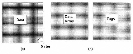
Figure 2.24
Data and tag area model. (a) shows the layout of a register set. (b)
shows a cache consisting of data array plus directory. |
|
|
|
|
|
|
|
|
Some of the more important parts of the chip for area modeling are the register set/cache/buffer areas of the chip, since these are the most frequent targets of design tradeoffs. The register set is an integral part of the data path of the system, but the total area that it occupies is not simply the number of bits that the register set stores. Register sets are usually referred to as dual or three-ported registers. They allow the user to access two words in one cycle and to return a value to a third word in the register set. Actually, these cells usually consist of one dedicated read port and a time-multiplexed read-and-write port, since the write occurs at the end of the cycle and the reads occur at the beginning of the cycle. These three-ported register buffers have both bit line sense amplifiers and control line drivers that occupy area in addition to the data array itself. It has been empirically determined [207] that the sense amplifiers and drivers add approximately six rbe to each dimension of the data buffer (Figure 2.24a). Thus, for a "three-ported" register set, we have the following area relationship: |
|
|
|
 |
|
|
|
|
Area of register = (number of regs + 6) (bits per reg + 6) rbe. |
|
|
|
|
|
|
|
|
A 16-word-by-32-bit register set has approximately 1.6 rbe per bit of data stored. If the same register set size were doubled to 32 words by 32 bits, it would have 1.4 rbe per data bit. |
|
|
|
|
|
|
|
|
Caches use smaller cells; thus, for cache storage using static cells, the following relationship has been determined [206]: |
|
|
|
|
|
|
|
|
Area of cache = 195 + 0.6K1(data bits) + 0.6K2 (tag bits) rbe, |
|
|
|
|
|
|
|
|
where 195 rbe is allocated to control (e.g., a small PLA), and K1 and K2 are area overhead associated with particular cache organizations. Each of K1 and K2 is of the form 1 + (cache parameters/cache size). As cache size increases, these overhead factors (K1, K2) asymptotically approach one [231]. |
|
|
|
|
|
|
|
|
As shown in Figure 2.24, caches include more than the data array. The cache must also allocate storage for address tags and other information such as dirty bits, valid bits, a comparator, and control logic (Figure 2.24b). These items are discussed in more detail in Chapter 5. |
|
|
|
|
|