|
|
|
|
|
|
|
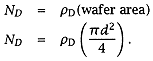
The yield can be determined as |
|
|
|
|
|
|
|
|
This describes a Poisson distribution of defects. |
|
|
|
|
|
|
|
|
so that if rD is the defect density per unit area, then |
|
|
|
|
|
|
|
|
For large wafers the diameter of the wafer is significantly larger than the die side and |
|
|
|
|
|
|
|
|
Figure 2.20 shows die yield as a function of rDA, the Poisson defect distribution. This is known to be a somewhat pessimistic model of yield; a more accurate estimate is also shown. For the processor designer, the issue is area. Doubling the area has significantly more effect on yield for already large rDA (i.e., » 510 or more). Thus, the large die designer gambles that technology will lower rD in time to provide a sufficient yield for a profitable product. |
|
|
|
|
|
|
|
|
Die cost is determined by area in two ways. One, as die area increases, fewer die are realized from a fixed size wafer. Two, as per our previous discussion, as the die area increases the yield decreases. This combination of effects is illustrated in the following example: |
|
|
|
|
|
|
|
|
Assume a wafer has diameter of 21 cm and costs $5,000 for a particular production run. Compute the cost per die for die area =2.3 cm2 and for 1 cm2 if rD = 1 defect/cm2. |
|
|
|
|
|