|
|
|
|
|
|
|
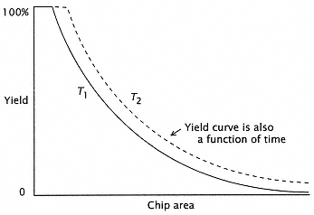
Figure 2.18
Yield vs. chip area at various points in time. |
|
|
|
|
|
|
|
|
Semiconductor technology has made significant advances in recent years. Both manufacturing and design processes have been improved. Improvements in the design process, largely due to improved photolithography, allow larger amounts of processor logic to be included in a constant area. Designs are limited by the resolution of the photolithography or the ability to define distinct geometries on the wafer surface. Because of optical resolution, and even the wavelength of light itself, devices, connections, etc., on a die have edge irregularities. Thus, the underlying feature that is produced must be large enough (have sufficient area) to insure correct operation. For this reason, the concept of minimum feature size, or geometric limit, is an important parameter to any designer. For our purposes, we may regard the minimum feature size as the minimum transistor length. The smaller the minimum feature size, the more transistors can be implemented in a given area. |
|
|
|
|
|
|
|
|
The area available to a designer, on the other hand, is largely a function of the manufacturing processing technology. This includes the purity of the silicon crystals, the absence of dust and other impurities, and the overall control of the diffusion and process technology. Improved manufacturing technology allows larger die to be realized with higher yields. Both photolithography technology and process technology are constantly improving. Processor designs are frequently not readily scalable to use these improvements. Rather, at a certain point a design team embarks on a completely new design to take advantage of improvements in technology. For the processor designer, there is a delicate design decision to be made early on: what die area and what lithography ought we to use to achieve a product with a maximum program life and maximum market impact? The conservative designer is not always a winner in this tradeoff. While the resultant (smaller) design may achieve excellent yields early in its product life, these yields generally will not improve much over product life and the design may be easily surpassed by competitive groups who wait a little longer and then have improved lithography or larger die area available to them for their designs. The successful designer must be aggressive enough in anticipating the movement of technology so that, although early designs may have |
|
|
|
|
|