|
|
|
|
|
|
|
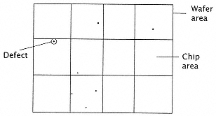
Figure 2.17
Defect distribution on a wafer. |
|
|
|
|
|
|
|
|
Almost all modern designs are based upon silicon technology in one or another VLSI format. Given a set of VLSI technology parameters, there are two primary determinants of cost: |
|
|
|
|
|
|
|
|
2. Silicon area occupied. |
|
|
|
|
|
|
|
|
It would not be inaccurate to look at the problem of modern processor design as a problem of dealing with islands of logic connected only by a limited number of connection paths, terminated through a limited number of pins and bonding pads. Since the bandwidth on these connections is limited, the total amount of data that can be transmitted is also limited. Regardless of how fast the logic executes, there remains an upper limit to the usefulness of the insular computation bounded by the communications bandwidth available for interchip communications. |
|
|
|
|
|
|
|
|
Most processors are implemented on one or a few chips, each housing a die about 1015 mm on a side. These die are produced in bulk from a larger wafer, perhaps 1521 cm in diameter (about 68 inches). Initially, the concern with limited chip area may seem unwarranted. One could simply expand the chip size and produce fewer chips on a wafer, and with these larger chips accommodate any desirable feature or function that the designer might wish to include. Unfortunately, neither the silicon wafers nor processing technologies are perfect. Defects randomly occur over the wafer surface (Figure 2.17). Large chip areas require an absence of defects over that area. If chips are too large for a particular processing technology, there will simply be no yield at all. Defects will be found on all the die on a particular wafer. Figure 2.18 illustrates yield vs. chip area. |
|
|
|
|
|
|
|
|
It is important to note that a good design is not necessarily one that immediately produces maximum yield. Reducing the area of a design below a certain critical amount has only a marginal effect on yield, which at that point is simply determined by the percentage area affected by defects. Additionally, small designs waste area because there is a required separation between adjacent die on a wafer, so smaller die size simply means a larger amount of area dedicated to interstitial unused wafer area. |
|
|
|
|
|