|
|
|
|
|
|
|
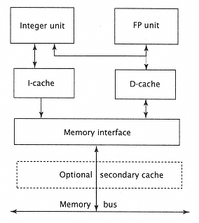
Figure 10.7
Baseline block diagram. |
|
|
|
|
|
|
|
|
Suppose we have just been told that our process engineers have derived an improved process which decreased the minimum feature size to 0.75m. We are given the task of designing the highest-performance microprocessor based on this new process. The instruction set is to remain unchanged to maintain software compatibility. Most modules of a baseline processor have been designed and used by a previous processor designed using a technology with 1m feature size. The only modifications allowed to these modules are data-path widths and controls. Our task is to efficiently use the additional transistors (area) available to us. A decision was made to consider three possible configurations with identical area and cycle time constraints: |
|
|
|
|
|
|
|
|
1. Single-issue processor (akin to our baseline) with a branch adder and expanded cache. The high-level block diagram is shown in Figure 10.7, and the processor organization is shown in Figure 10.8. |
|
|
|
|
|
|
|
|
2. Superscalar processor that inspects four instructions and issues up to two instructions every cycle. |
|
|
|
|
|
|
|
|
3. Two baseline processors, each possessing its own I-cache and sharing one D-cache. The high-level block diagram is shown in Figure 10.9. |
|
|
|
|
|
|
|
|
The key element of this study is selecting the optimum cache and memory organizations for each configuration. The best-performing measure in CPI is selected. An optional 256KB direct-mapped secondary cache is available with a cost increase of 20%. In order to justify the addition of secondary cache, the designers need to demonstrate an accompanying increase in performance of greater than 20%. |
|
|
|
|
|
|
|
|
The second objective of this study is to look at the optimum evolution path as one scales the technology. Along with the 0.75m feature size, we |
|
|
|
|
|