|
|
|
|
|
|
|
Figure 2.4
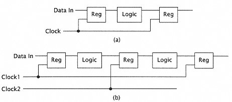
Single-rank, transparent clocking. |
|
|
|
|
|
|
|
|
Figure 2.5
Clocks. (a) Single phase. (b) Two-phase. |
|
|
|
|
|
|
|
|
The single-rank register is fast and has lower cost, but the dual-rank register has clocking advantages. It avoids the logical hazard caused when Pmin < tw. In the single-rank register (level-sensitive), it is possible for "fast path" data to arrive at the data input of the register while the clock is still enabled (during tw). This would cause no problem for the dual-rank register. |
|
|
|
|
|
|
|
|
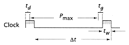
Figure 2.3 shows a conventional arrangement where a single phase clock is used to enter data into the register after it has transited the logic. Typically, the registers are of simple design; when the clock is high, data on the data in line is sampled into the register. The register is enabled by the clock in the case of a level-sensitive single-rank register. Such clocking must satisfy some constraints (Figure 2.3). |
|
|
|
|
|
|
|
|
First, the clock pulse width (tw) must be long enough both to ensure distribution across the entire system (pulse shrinkage is frequently a problem) and to ensure that the data-in is properly latched into the register when the clock is enabled (tw > register hold time). |
|
|
|
|
|
|
|
|
Second, the time between clock pulses, tm, must be sufficiently long to ensure that the worst possible logic path delay between any two registers is valid when the data-in is sampled at the receiving register (tm > Pmax). |
|
|
|
|
|
|
|
|
A third constraint is clock hazard: tw (the pulse width) must not be longer than the minimum possible path across the logic between two registers, Pmin. Otherwise, when such a path is enabled, new data being latched into the sending register is transmitted a cycle early into the receiving register (tw < Pmin). |
|
|
|
|
|
|
|
|
An alternative clocking technique is to use a multiphased clock. Here, multiple separate clock lines replace the single clock. These separate clock lines (actually, clock-phase lines) enable successive logic stages (Figure 2.5). The |
|
|
|
|
|