signal is stored in the input latch. When the clock is disabled, the output of the first latch is transferred to the output latch, and soon after is available as output data. The enabling or triggering mechanism can be either the clock level (level triggered) or the rise or fall transaction of the clock (edge triggered, Figures 2.2a and 2.2b).
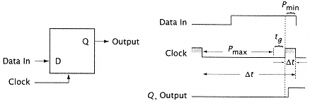
The clocking overhead is the additional delay in the worst-case delay path due to register delay and the clock. Suppose we define the following terms:
Pmax: maximum delay in logic without clock overhead (C)
Pmin: minimum delay in the shortest logic path
tw: clock pulse width
Dt: cycle time
tg: register data setup time
td: register output delay after data and clock are enabled
C: clock overhead
For a conventionally clocked system (Figure 2.1):
Dt = Pmax + C.
Figure 2.3 illustrates conceptual clocking for simple processors. The timing for C is:
C = tg + tw (assuming tw > d).
Most processors use a transparent clock (Figure 2.4). This clocking eliminates tw from C by moving the sample forward in the cycle by tw. This improves the clock overhead to:
C = tg + td,
while with a dual-rank edge-triggered clock, data enters rank one on the rising edge of the clock and is available at the output (rank two) on the falling edge. So: