|
|
|
|
|
|
|
Figure 2.6
Single-phase, level-sensitive clock. |
|
|
|
|
|
|
|
|
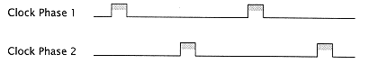
Figure 2.7
Two-phase, level-sensitive clock. |
|
|
|
|
|
|
|
|
design is arranged so that the two clocks do not overlap (Figure 2.7), and the logic is partitioned so that adjoining registers are clocked on separate phases of the clock. In a two-phase, level-sensitive clocking scheme, short paths cannot affect the proper entry of data into the register. Thus, only the first two constraints apply. |
|
|
|
|
|
|
|
|
With the transparent single-rank register and a single-or multi-phase clock, it is possible to propagate the register output data as soon as it is available, and begin a new "cycle"actually a clock phase. Thus, for this case |
|
|
|
 |
|
|
|
|
C = tg + td. |
|
|
|
|
|
|
|
|
If the arrival of the clock is not carefully controlled, a time ambiguity called uncontrolled clock skew is introduced. If the arrival time of the clock is ±d, then the clock period (cycle) must be extended by 2d (the sum of the earliest and latest deviations). This increases C to |
|
|
|
|
|
|
|
|
C = tg + td + 2d. |
|
|
|
|
|
|
|
|
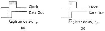
Single-rank, transparent clocking is preferred for most clocking arrangements, as it provides a minimum of complexity in the design and minimizes the clock overhead (Figure 2.8). Edge-triggered clocks are also used, and they also serve to minimize the fast path logical hazard. Such paths become a problem only when there is a significant amount of clock skew between the two registers. |
|
|
|
|
|
|
|
|
Most modern systems, both mainframe and microprocessors, use multiphase level-sensitive clocking. |
|
|
|
|
|
|
|
|
Figure 2.8
Level-sensitive (a) and edge-triggered (b) clocks acting
on registers (or latches). |
|
|
|
|
|