|
|
|
|
|
|
|
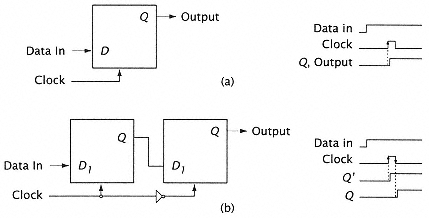
Figure 2.2
Edge-triggered clocks. (a) Single rank. (b) Dual rank. |
|
|
|
|
|
|
|
|
6. Data Fetch (DF) or Target Instruction Fetch (TIF): the cycles required to fetch the designated information from the memory system. |
|
|
|
|
|
|
|
|
7. Execute (EX): the cycles required to perform the operation designated by the instruction. |
|
|
|
|
|
|
|
|
8. Put Away (PA) or Writeback: the time to write a result in a designated register. Sometimes this action is included in the last EX cycle. |
|
|
|
|
|
|
|
|
Each of the preceding functional actions is allocated one or more processor cycles, although some of these functions may be concurrenttypically, decode and register fetch occur during the same cycle. For simple processors, the designer determines the time required for each functional event (the worst-case path through each functional unit) and then defines a cycle time based on (perhaps) the average of the various maximum functional times. Units that require more than this time are allocated multiple cycles. This may or may not be an optimum arrangement depending on the effects of quantization of cycle time on the other units. The goal is to minimize the overall instruction execution time. |
|
|
|
|
|
|
|
|
2.2.3 Clocking Overhead and Reliable Clocking |
|
|
|
|
|
|
|
|
The type of clockingthe way data is sampled into storage elementsis another important part of processor design. The clock is responsible for entering or sampling data into the register in a synchronously clocked system. The time between corresponding clock actions is the cycle time. |
|
|
|
|
|
|
|
|
Several variations of synchronous clocking are possible, depending on how data is sampled into the register and how the register is originally designed. Registers are of two basic forms (single rank and dual rank), and have two distinct clock triggering mechanisms (level triggered and edge triggered). A single-rank register transmits the input data to the output soon (perhaps two gate delays) after it has been enabled (triggered) by the clock (Figure 2.2a). A dual-rank register consists of two latchesan input and an output latch (Figure 2.2b). When the clock is initially enabled, the data-in |
|
|
|
|
|