|
|
|
|
|
|
|
the address in the PC by two byte positions to indicate the starting point of the next instruction. |
|
|
|
|
|
|
|
|
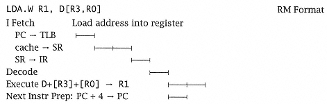
Note 2 Note that this instruction uses an RM format because it contains a register and a memory address. It does not use the memory address to access memory. We assume RO contains zero. |
|
|
|
|
|
|
|
|
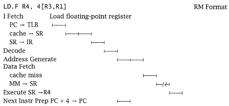
Note 3 The data address generate includes time to access the TLB. A cache miss occurs presumably because this is the first reference to the data region. It is assumed that subsequent data references are in the cache. |
|
|
|
|
|