|
|
|
|
|
|
|
1.8.1 Examples of Well-mapped Machine Instruction Timing |
|
|
|
|
|
|
|
|
The examination of a machine is not unlike the examination of the insides of a mechanical watch: it is easy to be overwhelmed by the detail, yet over 90% of the process execution time is spent using only a few data paths in very ordinary ways. It is the attempt here to bring simplicity and understanding to the execution process rather than to provide absolute completeness. Therefore, details such as setting up the condition code, memory bounds checking, interrupt checking, etc., are omitted. Actions are fit into the designated cycles. Only the most essential data paths are shown and only the most common instructions are evaluated. We assume that the cycle time has already been established. |
|
|
|
|
|
|
|
|
Study 1.1 Performance Evaluation |
|
|
|
|
|
|
|
|
For the following two problems assume a well-mapped R/M processor with the data paths as shown in Figure 1.25. The cache access time is two cycles (one for directory, one for array access). The cache miss time is six cycles (one for cache directory access and five to access memory). It takes two cycles (abbreviated by "~" hereafter) to generate the address (1 ~ to calculate address, (1 ~ for TLB). Also, assume there are no TLB misses. |
|
|
|
|
|
|
|
|
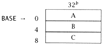
1. (a) Write the R/M code to execute the statement |
|
|
|
|
|
|
|
|
where A, B, and C are normalized, short floating-point numbers (.F) resident in memory. Assume the BASE address is memory address #D. |
|
|
|
 |
|
|
|
|
SUB R3,R3 ;zero index register
LDA.W R1, 0D[R3,R0] ;load inst R1 with BASE
LD.F R4, 04[R3,R1] ;load B
ADD.F R4, 08[R3,R1] ;add C
ST.F 0[R3,R1], R4 ;store result in A |
|
|
|
|
|
|
|
|
(b) Develop the detailed instruction timing for the code in problem (a). Assume both code and data are resident in main memory and ALU execution requires two cycles. |
|
|
|
|
|