|
|
|
|
|
|
|
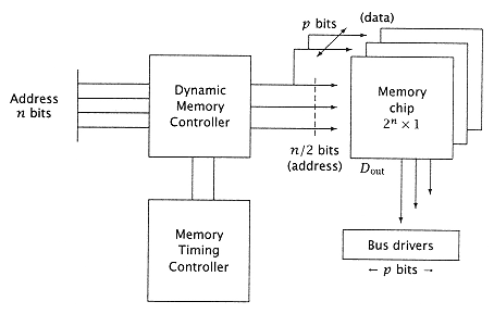
Figure 6.6
A memory module; some typical memory parameters are described in
Appendix D. |
|
|
|
|
|
|
|
|
Since the Dynamic Memory Controller output drives all p bits, and hence p chips, of the physical word, the controller output may also require buffering. As the memory read operation is completed, the data-out signals are directed at bus drivers which then interface to the memory bus, which is the interface for all of the memory modules. |
|
|
|
|
|
|
|
|
The access and cycle time of the module differs from the chip access and cycle times. The module access time must now include the delay in multiplexing the address lines in the dynamic memory controller as well as the memory chip access time and any delay in transitioning through the output bus drivers. Since data access can be pipelined in a synchronous memory module, the cycle time is less affected by this peripheral circuitry than the access time. In larger memory systems, the cycle time for the module and the system remains relatively similar to the chip cycle time, while the access time is a direct function of the total size of the memory system. |
|
|
|
|
|
|
|
|
Two important features found on a number of memory chips directly affect the design of the memory system. These features are called: |
|
|
|
|
|
|
|
|
Both of these are techniques for improving the transfer rate of memory words. In nibble mode, a single address (row and column) is presented to the memory chip and the CAS line is toggled repeatedly. Internally, the chip interprets this CAS toggling as a mod 2w progression of low-order column addresses. Thus, sequential words can be accessed at a higher rate from the memory chip. For example, for w = 2, we could access four consecutive low-order bit addresses, e.g.: |
|
|
|
|
|