|
|
|
|
|
|
|
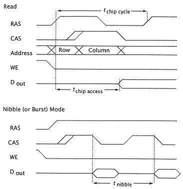
Figure 6.5
Memory chip timing. |
|
|
|
|
|
|
|
|
impedance state until it is activated either high or low depending on the contents of the selected memory cell. |
|
|
|
|
|
|
|
|
The time from the beginning of RAS until the data output line is activated is a very important parameter in the memory module design. This is called the chip access time or tchip access. The other important chip timing parameter is the cycle time of the memory chip (tchip cycle.). This is not the same as the access time, as the selected row and column lines must recover before the next address can be entered and the read process repeated. Thus, the tchip cycle is determined by the amount of time that the RAS line is active and the minimum amount of time that the RAS must remain inactive to allow the chip and the sense amplifiers to fully recover in preparation for the next read. |
|
|
|
|
|
|
|
|
The memory module does not simply consist of memory chips (Figure 6.6). In a memory system with p bits per physical word, and 2n words in a module, the n address bits enter the module and are usually directed at a Dynamic Memory Controller chip. This chip in conjunction with a Memory Timing Controller provides the following functions: |
|
|
|
|
|
|
|
|
1. Multiplex of the n address bits into a row and a column address for use by the memory chips. |
|
|
|
|
|
|
|
|
2. The creation of the correct RAS and CAS signal lines at the appropriate time. |
|
|
|
|
|
|
|
|
3. Provide timely refresh of the memory system. |
|
|
|
|
|