|
|
|
|
|
|
|
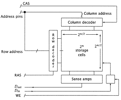
Figure 6.4
A memory chip. |
|
|
|
|
|
|
|
|
With large-sized memories, the number of address lines dominates the pinout of the chip. In order to conserve these pins and provide a smaller package for better overall density, the row and column addresses are multiplexed onto the same lines (input pins) for entry onto the chip. Two additional lines are important here: RAS (row address strobe) and CAS (column address strobe). These gate first the row address, then the column address into the chip. The row and column addresses are then decoded to select one out of the 2n/2 possible lines. The intersection of the active row and column lines is the desired bit of information. The column line's signals are then amplified by a sense amplifier and transmitted to the output pin (data out, or Dout) during a read cycle. During a write cycle, the write-enable signal stores the data-in (Din) signal to specify the contents of the selected bit address. |
|
|
|
|
|
|
|
|
All of these actions happen in a sequence approximated in the timing diagram in Figure 6.5. At the beginning of a read from memory, the RAS line is activated. With the RAS active and the CAS inactive, the information on the address lines is interpreted as the row address and stored into the row address register. This activates the row decoder and the selected row line in the memory array. The CAS is then activated, which gates the column address lines into a column address register. Note that: |
|
|
|
|
|
|
|
|
1. The two rise times on CAS represent the earliest and latest that this signal may rise with respect to the column address signals. |
|
|
|
|
|
|
|
|
2. WE is write enable. This signal is inactive during read operations. |
|
|
|
|
|
|
|
|
The column address decoder then selects a column line; at the intersection of the row and column line is the desired data bit. During a read cycle the write enable is inactive (low) and the output line (Dout) is at a high- |
|
|
|
|
|