|
|
|
|
|
|
|
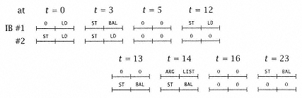
Figure 4.30
Contents of the I-buffers. |
|
|
|
|
|
|
|
|
A plausible timing for the study code is shown in Figure 4.31. At t = 0, we assume that the first three instructions are already in the two IB words, as shown. At t = 1 the (first) LD instruction passes into the decoder and an IF begins to fetch the next eight bytes of instruction into IB #1. This completes at t = 3, when instructions 4 and 5 are now in IB #1. When the address generate (AG) and translate (T) completes for instruction 2 (ST), it is found that the destination is within a few bytes of the current instruction. Since this is an unusual occurrence, further checking is not done; rather, the current contents of the IB (#1 and #2) are declared invalid and are to be refetched when the store has completed (at the end of t = 9). The IF ® IB1 refetches the ST and LD instructions during cycles 10 and 11. Another IF brings the ST and BAL into IB2. The LD is decoded in cycle 12, freeing IB1 (and fetching the contents of ARGLIST into IB1 by cycle 14). Again, at the end of cycle 15, a potential store into the instruction buffer is detected and the IB is invalidated. The store completes in cycle 20, and again (cycles 21 and 22) a final fetch into the IB allows the BAL to be decoded. |
|
|
|
|
|
|
|
|
Study 4.11 Evaluating the Performance of the Baseline Microprocessor |
|
|
|
|
|
|
|
|
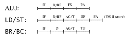
In this study, we look at the performance of the processor outlined in study 2.3. Our baseline microprocessor is a straightforward design using an L/S instruction set. We assume for the moment that, as is current practice, we have a short pipeline. For the moment, we do not use branch enhancement techniques such as I-buffers, etc. We have the following timing templates: |
|
|
|
|
|
|
|
|
We assume that the register file is accessed during the decode cycle and hence the values are available for either address generation or execution in the cycle following the decode cycle. We also assume that address generation and translation can be done in a single cycle. This is common practice in less aggressive L/S microprocessor designs. More aggressive designs will increase the total number of execution cycles and achieve significantly |
|
|
|
|
|