|
|
|
|
|
|
|
Figure 4.5
The MIPS R2000 microprocessor. |
|
|
|
|
|
|
|
|
Figure 4.6
The MIPS R4000 microprocessor. |
|
|
|
|
|
|
|
|
Figure 4.7
The IBM RS 6000 microprocessor. |
|
|
|
|
|
|
|
|
(one "cycle" in R2000 terms; two cycles or actions in our terms); see Figure 4.5. |
|
|
|
|
|
|
|
|
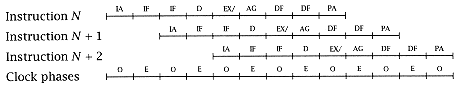
The MIPS R4000 processor also uses a two-phase clock, only here a new instruction is issued each clock phase. On a LD/ST the EX is replaced by AG. On an ALU instruction the template allows four EX (half) cycles before PA is delayed. The C (half) cycle is for a cache tag check (Figure 4.6). |
|
|
|
|
|
|
|
|
This machine can, under certain conditions, issue multiple instructions in a single cycle, and is discussed further in Chapter 7. The determination of which instructions are to be issued is made in the DI (dispatch) stage. In an LD/ST, the EX is replaced with AG and PA with DF. If only one instruction were issued in each cycle, we would have the timing template shown in Figure 4.7. |
|
|
|
|
|
|
|
|
The HP PA-RISC has a conventional L/S timing template, but is known for aggressive technology implementations with high clock rates. In the LD/ST instructions, the first EX is replaced with AG and the second does the Dcache read (Figure 4.8). Most ALU operations use only the first EX. |
|
|
|
|
|
|
|
|
Figure 4.8
The HP PA-RISC 1.1 microprocessor. |
|
|
|
|
|