|
|
|
|
|
|
|
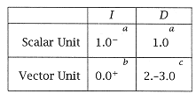
a Nominally. Reduced by I-buffer, I-cache. |
|
|
|
|
|
|
|
|
b Relatively small compared to other requirements. |
|
|
|
|
|
|
|
|
c Minimum required is one VLD and one VST concurrently; preferably two VLD's and one VST, all concurrently. |
|
|
|
|
|
|
|
|
7.12 and 7.13, is called chaining. It is illustrated in Figure 7.12 by a chained ADD-MPY with each functional unit having 4 stages. If the ADD-MPY were unchained, it would take 4 (startup) + 64 (elements/VR) = 68 cycles for each instruction136 cycles total. With chaining, this is reduced to 4 (add startup) + 4 (multiply startup) + 64 (elements/VR) = 72 cycles. |
|
|
|
|
|
|
|
|
One of the crucial aspects to achieving the performance potential of the vector processor is the management of references to memory. Since arithmetic operations complete one per cycle, a vector code makes repeated references to memory to introduce new vectors in the vector registers and to write out old results. Thus, on the average memory must have sufficient bandwidth to support at least a two-words-per-cycle execution rate (one read and one write), and preferably three references per cycle (two reads and one write). This bandwidth allows for two vector reads and one vector write to be initiated and executed concurrently with the execution of a vector arithmetic operation. If there is insufficient memory bandwidth from memory to the vector registers, the processor necessarily goes idle after the vector operation until the vector loads and stores are complete. It is a significant challenge to the designer of a processor not to simply graft a vector processing extension onto a scalar processor design, but rather to adapt the scalar designespecially the memory systemto accommodate the requirements of fast vector execution (Table 7.1). If the memory system bandwidth is insufficient, the designer will find that there is correspondingly less performance improvement from the vector processing hardware. |
|
|
|
|
|
|
|
|
7.2.4 A Generic Vector Processor |
|
|
|
|
|
|
|
|
We can now bring the major elements of the vector processor together (Figure 7.14). The functional units (add, multiply, etc.) and the two register sets (vector and scalar, or general) are connected by one or more bus sets. If chaining (Figure 7.13) is allowed, then three (or more) source operands are simultaneously accessed from the vector registers and a result is transmitted back to the vector registers. Another bus couples the vector registers and the memory buffer. The remaining parts of the systemI-cache, D-cache, general registers, etc.are typical of pipelined processors. |
|
|
|
|
|