For this study, we assume a simple timing template with an R/M: S/390-type instruction format.
In this study, we examine the control logic required to interlock a pipelined processor, as well as the extra logic needed to allow for a bypass of the needed data, which reduces the delay. The problem is to design the logic for the address generation interlock, and then to add the bypass logic.
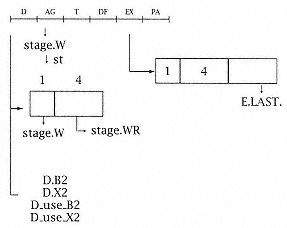
We assume a design typical of a pipelined R/M architecture with a pipeline structure as shown in Figures 4.28 and 4.29. The stages operate as follows:
D Decode instruction and read registers for address generation. There are 16 GPRs, each 32 bits wide. Depending on the type of instruction, address generation may or may not be required; if it is, it may require one or two registers.
AG Generate the logical operand address (3-input adder).
T TLB to translate to a real address.
DF Fetch operand from cache and align as needed.
EX Execute the function. Execution may take one or many cycles; on "run-on" (EX of more than one cycle), the E-unit interlocks other operations until it is done. The E-unit always "knows" when it is in the last cycle of execution at the beginning of that cycle.
PA Write results to register file or store buffer.
Recall the R/M instruction (S/390) layout is as follows: